
Research Topics - ISGE
- Silicon power devices and integration
- Wide bandgap (GaN, SiC, Diamond) power devices and integration
- Systems for power conversion and management (photovoltaic, multi-sources)
- Software defined converters
- Reliability and robustness with respect to severe environment (electrostatic discharges, radiations)
Monolithic integration of switching cells
This research activity aims at developing a more integrated and compact power electronics (breakdown voltage 1200 V and current density 100 A/cm2) obtained by the emergence of new monolithic structures and mixed monolithic-hybrid in the form of a network of switching cells and thus allowing to improve performance, reliability and to reduce fabrication cost as compared to the hybrid integration approach. The main objective is to demonstrate through technological realisations, and by following two original integration approaches, the monolithic integration in silicon of a generic static power converter (AC/DC or DC/AC) dedicated for medium power applications. The first integration approach called « dual chip » (figure 1) makes use of two generic and complementary monolithic power chips. One chip is a common anode monolithic multi-pole power chip that integrates the switches that share the anode electrode and form the high-side part of the converter. The other chip is a common cathode monolithic multi-pole power chip that integrates the switches that share the cathode electrode and form the low-side part of the converter. The second integration approach called a single chip or ultimate approach (figure 2) integrates all the switches (high-side as well as low-side) in a single chip. The objectives of the two approaches are the suppression of wire bonds and the reduction of parasitic capacitances in order to improve reliability and electrical performance.

Figure 1. Dual chip integration approach

Figure 2. Single chip monolithic integration approach
The first realised inverter is given on figure 3. This H-bridge is obtained by assembling on a PCB substrate a common anode three-pole chip, that integrates monolithically two RC-IGBT structures, and two discrete RC-IGBT chips that are mounted using the flip chip technique (cathode in contact with the PCB). The different power chips were realized using the IGBT technology process at the micro and nanotechnology platform in the Laboratory of Analysis and Architectures (LAAS).
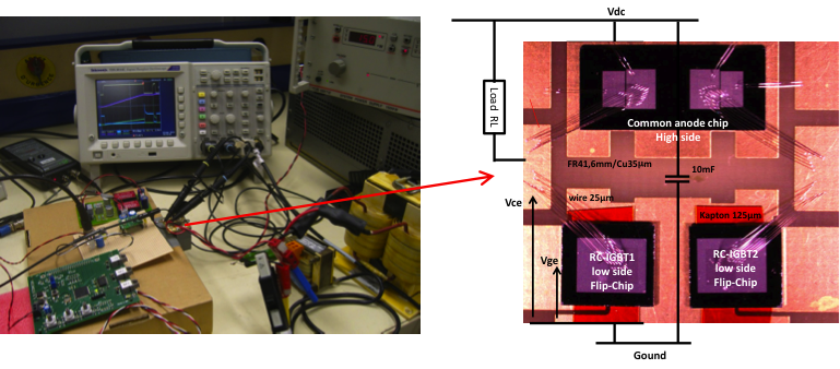
Figure 3. Experimental characterisation of the first realised inverter (H-bridge)
AC switches for specific mains applications
The management of electrical energy in the household applications (lighting, household appliances…) is an important market for the manufacturers of power semiconductor switching devices. In this field, the triac is widely used due to its reliability, low losses and low fabrication cost. However, the triac has some drawbacks in some applications like the « classical dimmer circuit » which is not compatible with most of electronic ballasts (capacitive load) mainly for low power ranges (˂ 100 W) and therefore low load currents (CFL, LED). In order to overcome this issue, dimmers based on the anti-series association of two MOS or IGBT devices are used. However, despite the improvements brought by these unidirectional devices, their high fabrication cost and the difficulty to implement the associated driver limit their widespread diffusion in this market. The devices that we are developing in this context are monolithic bidirectionnal devices controllable to turn-on and turn-off with respect to a single electrode reference and are intended for specific applications in which the load current is about 0,5A rms and the on-state voltage drop lower than 1V. The breakdown voltage of these devices is about 600V.
The technological realisation of the devices relies on the IGBT technology process of the micro and nanotechnology platform at LAAS. Specific technological steps such as the vertical P+ wall will be developed and integrated in the IGBT process flow.
Contacts: M. Breil, A. Bourennane, J-P. Laur
Wide bandgap (GaN, SiC, Diamond) power devices and integration
In the same way silicon technologies revolutionized computing and communication, silicon and semiconductors in general will play a key role in the emerging energy economy of the 21st century for the transmission, distribution and consumption of electricity. Major goals are still a significant improvement in energy efficiency and the development of the new generations of devices that are needed for more electric transports, for example. Device power integration activity will mainly focus on wide band gap high voltage and high temperature power devices. Our expertise in design, realisation and characterisation of silicon power devices is a main advantage and allows to rise the challenges related both to the design of novel architectures and to key technology steps required for their realisation and integration. These activities are developed with many collaborators in France but also in Europe, in particular in the International Associated Laboratory (LIA) WIDE-Lab (Wide Band gap technologies for Integration of Energy efficient Devices). Thanks to the European dimension offered by the three actors: Ampère, CNM and LAAS, WIDE-Lab creates a unique platform in the field of Wide Band Gap technologies and system integration.
GaN HEMT and Si/GaN Co-Integration
Our research activities on gallium nitride power switches are recent. During the years 2001-2005, one could note the substantial progress but primarily limited to normally-on power devices (mainly HEMT). Thus, the semiconductor technology evolutions make it possible to consider gallium nitride as a promising material, which deserves a true R&D investment. Furthermore, contrary to silicon carbide which must be carried out by crystalline growth on of the same substrate composition, GaN can be deposited by hetero-epitaxy on silicon substrates thus allowing a production on sections of more important surface (150 TO 200 mm).
Over the next few years, regarding the architecture GaN-based devices, we will thoroughly study the preliminary solutions we proposed for a normally-off device (2 patents were recently deposited in this way). We will not only focus on the basic switch but also work on the integration of several switches thanks to the co-integration of GaN and Si devices on the same Si substrate, so as to take advantage of the best features of both materials. This will allow the realisation of monolithically integrated functions, for instance cascode associations of GaN HEMT and a Si MOSFET (or Si Schottky diode) or multi-switches chips, such as a basic switching cell and a H-bridge.
Diamond Power Devices
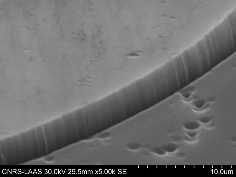
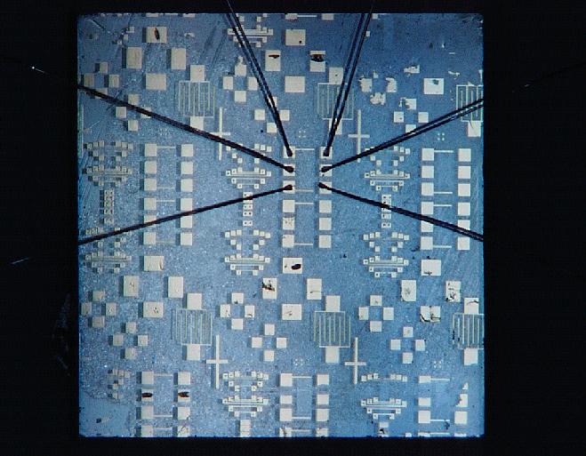
Thanks to its exceptional physical properties, diamond is the ideal material for power electronics. Since 2007, a consortium with the LAAS and the other laboratories and the companies, has the objective to develop the industry of the diamond in France through federative projects (DIAMONIX, DIAMONIX2). In the framework of these projects, demonstrators including Schottky diodes have been realised, in the LAAS technological platform and were able to confirm the diamond potential for high voltage and high temperature applications. The LAAS knowledge in silicon technology helps to develop basic technological steps required to the realisation of p-type diamond Schottky diode, such as:
|
|
|
SEM photograph of side of etched struture with CF4-O2 process | Characterisation device on P- diamond substrate (3*3mm²) |
A specific simulation platform with TCAD Sentaurus tools is also developed to design diamond power devices. This platform is particularly useful to design an advanced high voltage junction termination structures of diamond Schottky diodes, these periphery protections can be applied to the devices based on wide band gap materials such as GaN or SiC.
Despite the technological barriers related to the quality of the material and the size of the samples, we will continue to work on the PN junction with our partners, which is real technological obstacle to achieve diamond power devices. In the coming years, we will address the ambitious challenge of the diamond MOSFET realisation. The main task will be to develop key technology steps to achieve to achieve MOS capacitors on N-doped diamond, device ever conducted to date, and also on P-doped diamond.
Contacts : F. Morancho, K. Isoird, H. Scheider, P. Austin
Systems for power conversion and management (photovoltaic, multi-sources)
TODO
Contacts : TODO
Software defined converters
Power electronics is the key technology controlling electric energy flows across all applications in the world. From drones to data centers and through electric cars, the flow of energy is regulated, controlled and provided by power electronics devices. This makes power electronics an important aspect of any emerging technology business across the globe and a key to a successful energy transition.
Power electronics is extremely difficult to master. It is a multi-disciplinary field covering power devices, metrology, electronics, industrial informatics, control theory, data treatment to list only a few. It takes years of training for a power electronics engineer to be operational in the field and even longer for new products to become mature. This high-cost entry ticket is a major issue blocking bottom-up innovation on energy management throughout the world.
The Power electronics industry provides turn-key solutions which are tailored to fit local needs that were evaluated at a certain point in time. As these needs change with the market, the capital invested in the previous solutions is lost as these become obsolete. Over time, this creates a steady flow of power electronics waste with equipment that is still operational.
It is paramount to create a means to democratize access to power electronics which not only enables practitioners to quickly understand the technology and adapt it to their needs, but also to grant power electronics a much longer life span.
This research axis focuses on democratizing the access to power electronics by creating an integrated, open-source and free technology framework. This framework will be constituted of:
- a standardized hardware: will allow users to quickly deploy their solution and secure their initial investment by either reusing or stacking modules as the needs change with the market
- a simplified and intuitive development environment which will allow users to quickly deploy ready-made solutions or drastically lower the time it takes to develop a new one
- an open data management center which will give users the possibility to easily deploy advanced features, such as remote billing or preventive maintenance, or create new business models with their data.
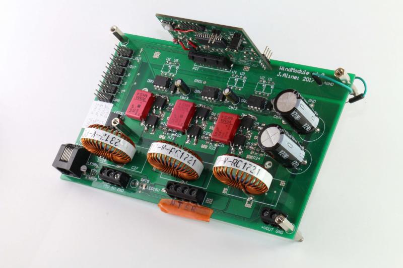
Figure 1: Power Electronics module under development at LAAS-CNRS
The technology framework and community services will be made available for free. The OwnTech project may eventually evolve into a company that will sell hardware and consulting projects, but the technology framework and the community services will remain free. Check ou plus de details on www.owntech.org
Contacts : Luiz Villa
Reliability and robustness with respect to severe environment (electrostatic discharges, radiations)
Power management systems are critical blocks to deliver the energy required by electronic circuits. Their safety is key for critical systems like (break assist and cruise control in automobiles, battery charger…) and it is thus required to optimize their robustness to obtain high reliability product. However this becomes more and more challenging with technologies evolution. Indeed, technological dimension reduction of integrated circuits and cohabitation of power units with their control logic on the same die tends to make it more and more difficult to maintain an acceptable level of robustness.
To address these critical issues we study the physics of circuits subjected to harsh environment that could impair their reliability, mainly:
- threats from the near environment : ElectroStatic Discharge (ESD)
- threats from the far environment: radiation
- ...
Based on the understanding of the phenomenon thanks to experimental measurements or simulations, we study and propose optimization to increase system immunity or provide effective protection solutions.
Contacts: P. Austin, D. Trémouilles
Contact
- Address: 7, avenue du Colonel Roche BP 54200 31031 Toulouse cedex 4, France
- GPS: Lat: 43.564330 | Long: 1.476839
- Phone: +33 (0) 5 61 33 62 00